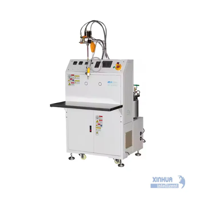
? Potting Process Overview:
-
Preparation:
- The PCB is cleaned and dried to remove dust, moisture, or contaminants.
- Sensitive areas that shouldn't be covered (e.g., connectors) are masked.
-
Mixing the Potting Compound:
- A resin (commonly epoxy, polyurethane, or silicone) is mixed with its hardener.
- Optional additives (like colorants or fillers) may be included.
-
Dispensing:
- The liquid resin is poured, injected, or dispensed into a mold or enclosure containing the PCB.
- Vacuum or pressure may be used to eliminate air bubbles.
-
Curing:
- The resin is left to harden at room temperature or under heat.
- Curing time and temperature depend on the resin type.
-
Finishing:
- Once cured, the PCB is removed from any molds or clamps.
- Masking is removed, and the unit is ready for use or further assembly.
✅ Benefits of Potting:
- Moisture resistance (waterproofing)
- Vibration and shock protection
- Chemical and corrosion resistance
- Electrical insulation
- Tamper resistance and IP rating enhancement
⚠️ Common Potting Materials:
| Material | Properties | Typical Use |
|---|---|---|
| Epoxy | Rigid, strong, high chemical resistance | Harsh environments, industrial |
| Polyurethane | Flexible, good for shock and vibration | Automotive, low-temp electronics |
| Silicone | High temp resistance, flexible | Aerospace, high-temp electronics |